MemTest86 V10.4 Pro Build: 1000
PassMark Software
www.passmark.com
Memory summary:
Number of RAM slots: 4
Number of RAM modules: 4
Number of RAM SPDs detected: 4
Total Physical Memory: 49124M
SPD Details:
--------------
SPD #: 0
==============
RAM Type: DDR3
Maximum Clock Speed (MHz): 933 (JEDEC)
Maximum Transfer Speed (MHz): DDR3-1867
Maximum Bandwidth (MB/s): PC3-14900
Memory Capacity (MB): 16384
Jedec Manufacture Name: SK Hynix
SPD Revision: 1.2
Registered: Yes
ECC: Yes
SPD #: 0
Manufactured: Week 45 of Year 2013
Module Part #: HMT42GR7AFR4C-RD
Module Revision: 0x5438
Module Serial #: 0x186A6447
Module Manufacturing Location: 0x01
# of Row Addressing Bits: 16
# of Column Addressing Bits: 11
# of Banks: 8
# of Ranks: 2
Device Width in Bits: 4
Bus Width in Bits: 64
Module Voltage: 1.5V
CAS Latencies Supported: 6 7 8 9 10 11 13
Timings @ Max Frequency (JEDEC): 13-13-13-32
Maximum Clock Speed (MHz): 933
Maximum Transfer Speed (MHz): DDR3-1867
Maximum Bandwidth (MB/s): PC3-14900
Minimum Clock Cycle Time, tCK (ns): 1.071
Minimum CAS Latency Time, tAA (ns): 13.125
Minimum RAS to CAS Delay, tRCD (ns): 13.125
Minimum Row Precharge Time, tRP (ns): 13.125
Minimum Active to Precharge Time, tRAS (ns): 34.000
Minimum Row Active to Row Active Delay, tRRD (ns): 5.000
Minimum Auto-Refresh to Active/Auto-Refresh Time, tRC (ns): 47.125
Minimum Auto-Refresh to Active/Auto-Refresh Command Period, tRFC (ns): 260.000
DDR3 Specific SPD Attributes
Write Recover Time, tWR (ns): 15.000
Internal Write to Read Command Delay, tWTR (ns): 7.500
Internal Read to Precharge Command Delay, tRTP (ns): 7.500
Minimum Four Activate Window Delay (ns): 27.000
RZQ / 6 Supported: Yes
RZQ / 7 Supported: Yes
DLL-Off Mode Supported: Yes
Maximum Operating Temperature Range (C): 0-95C
Refresh Rate at Extended Operating Temperature Range: 2X
Auto-Self Refresh Supported: No
On-die Thermal Sensor Readout Supported: No
Partial Array Self Refresh Supported: No
Thermal Sensor Present: Yes
Non-standard SDRAM Type: Standard Monolithic
Module Type: RDIMM
Module Height (mm): 29 - 30
Module Thickness (mm): front 1-2 , back 1-2
Module Width (mm): 133.5
Reference Raw Card Used: Raw Card E Rev. 2
DRAM Manufacture: SK Hynix
# of DRAM Rows: 2
# of Registers: 1
Register Manufacturer: IDT
Register Type: SSTE32882
Register Revision: 0x63
Command/Address A Outputs Drive Strength: Moderate Drive Command/Address B Outputs Drive Strength: Moderate Drive Control Signals A Outputs Drive Strength: Moderate Drive Control Signals B Outputs Drive Strength: Moderate Drive Y1/Y1# and Y3/Y3# Clock Outputs Drive Strength: Moderate Drive Y0/Y0# and Y2/Y2# Clock Outputs Drive Strength: Moderate Drive
SPD #: 1
==============
RAM Type: DDR3
Maximum Clock Speed (MHz): 933 (JEDEC)
Maximum Transfer Speed (MHz): DDR3-1867
Maximum Bandwidth (MB/s): PC3-14900
Memory Capacity (MB): 16384
Jedec Manufacture Name: SK Hynix
SPD Revision: 1.2
Registered: Yes
ECC: Yes
SPD #: 1
Manufactured: Week 45 of Year 2013
Module Part #: HMT42GR7AFR4C-RD
Module Revision: 0x5438
Module Serial #: 0x187A644F
Module Manufacturing Location: 0x01
# of Row Addressing Bits: 16
# of Column Addressing Bits: 11
# of Banks: 8
# of Ranks: 2
Device Width in Bits: 4
Bus Width in Bits: 64
Module Voltage: 1.5V
CAS Latencies Supported: 6 7 8 9 10 11 13
Timings @ Max Frequency (JEDEC): 13-13-13-32
Maximum Clock Speed (MHz): 933
Maximum Transfer Speed (MHz): DDR3-1867
Maximum Bandwidth (MB/s): PC3-14900
Minimum Clock Cycle Time, tCK (ns): 1.071
Minimum CAS Latency Time, tAA (ns): 13.125
Minimum RAS to CAS Delay, tRCD (ns): 13.125
Minimum Row Precharge Time, tRP (ns): 13.125
Minimum Active to Precharge Time, tRAS (ns): 34.000
Minimum Row Active to Row Active Delay, tRRD (ns): 5.000
Minimum Auto-Refresh to Active/Auto-Refresh Time, tRC (ns): 47.125
Minimum Auto-Refresh to Active/Auto-Refresh Command Period, tRFC (ns): 260.000
DDR3 Specific SPD Attributes
Write Recover Time, tWR (ns): 15.000
Internal Write to Read Command Delay, tWTR (ns): 7.500
Internal Read to Precharge Command Delay, tRTP (ns): 7.500
Minimum Four Activate Window Delay (ns): 27.000
RZQ / 6 Supported: Yes
RZQ / 7 Supported: Yes
DLL-Off Mode Supported: Yes
Maximum Operating Temperature Range (C): 0-95C
Refresh Rate at Extended Operating Temperature Range: 2X
Auto-Self Refresh Supported: No
On-die Thermal Sensor Readout Supported: No
Partial Array Self Refresh Supported: No
Thermal Sensor Present: Yes
Non-standard SDRAM Type: Standard Monolithic
Module Type: RDIMM
Module Height (mm): 29 - 30
Module Thickness (mm): front 1-2 , back 1-2
Module Width (mm): 133.5
Reference Raw Card Used: Raw Card E Rev. 2
DRAM Manufacture: SK Hynix
# of DRAM Rows: 2
# of Registers: 1
Register Manufacturer: IDT
Register Type: SSTE32882
Register Revision: 0x63
Command/Address A Outputs Drive Strength: Moderate Drive Command/Address B Outputs Drive Strength: Moderate Drive Control Signals A Outputs Drive Strength: Moderate Drive Control Signals B Outputs Drive Strength: Moderate Drive Y1/Y1# and Y3/Y3# Clock Outputs Drive Strength: Moderate Drive Y0/Y0# and Y2/Y2# Clock Outputs Drive Strength: Moderate Drive
SPD #: 2
==============
RAM Type: DDR3
Maximum Clock Speed (MHz): 933 (JEDEC)
Maximum Transfer Speed (MHz): DDR3-1867
Maximum Bandwidth (MB/s): PC3-14900
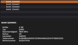
Memory Capacity (MB): 8192
Jedec Manufacture Name: Samsung
SPD Revision: 1.2
Registered: Yes
ECC: Yes
SPD #: 2
Manufactured: Week 6 of Year 2015
Module Part #: M393B1G70QH0-CMA
Module Revision: 0x0000
Module Serial #: 0x13515B30
Module Manufacturing Location: 0x03
# of Row Addressing Bits: 16
# of Column Addressing Bits: 11
# of Banks: 8
# of Ranks: 1
Device Width in Bits: 4
Bus Width in Bits: 64
Module Voltage: 1.5V
CAS Latencies Supported: 6 7 8 9 10 11 13
Timings @ Max Frequency (JEDEC): 13-13-13-32
Maximum Clock Speed (MHz): 933
Maximum Transfer Speed (MHz): DDR3-1867
Maximum Bandwidth (MB/s): PC3-14900
Minimum Clock Cycle Time, tCK (ns): 1.071
Minimum CAS Latency Time, tAA (ns): 13.125
Minimum RAS to CAS Delay, tRCD (ns): 13.125
Minimum Row Precharge Time, tRP (ns): 13.125
Minimum Active to Precharge Time, tRAS (ns): 34.000
Minimum Row Active to Row Active Delay, tRRD (ns): 5.000
Minimum Auto-Refresh to Active/Auto-Refresh Time, tRC (ns): 47.125
Minimum Auto-Refresh to Active/Auto-Refresh Command Period, tRFC (ns): 260.000
DDR3 Specific SPD Attributes
Write Recover Time, tWR (ns): 15.000
Internal Write to Read Command Delay, tWTR (ns): 7.500
Internal Read to Precharge Command Delay, tRTP (ns): 7.500
Minimum Four Activate Window Delay (ns): 27.000
RZQ / 6 Supported: Yes
RZQ / 7 Supported: Yes
DLL-Off Mode Supported: Yes
Maximum Operating Temperature Range (C): 0-95C
Refresh Rate at Extended Operating Temperature Range: 2X
Auto-Self Refresh Supported: No
On-die Thermal Sensor Readout Supported: No
Partial Array Self Refresh Supported: No
Thermal Sensor Present: Yes
Non-standard SDRAM Type: Standard Monolithic
Module Type: RDIMM
Module Height (mm): 29 - 30
Module Thickness (mm): front 1-2 , back 1-2
Module Width (mm): 133.5
Reference Raw Card Used: Raw Card C Rev. 2
DRAM Manufacture: Samsung
# of DRAM Rows: 1
# of Registers: 1
Register Manufacturer: IDT
Register Type: SSTE32882
Register Revision: 0x63
Command/Address A Outputs Drive Strength: Moderate Drive Command/Address B Outputs Drive Strength: Moderate Drive Control Signals A Outputs Drive Strength: Moderate Drive Control Signals B Outputs Drive Strength: Moderate Drive Y1/Y1# and Y3/Y3# Clock Outputs Drive Strength: Moderate Drive Y0/Y0# and Y2/Y2# Clock Outputs Drive Strength: Moderate Drive
SPD #: 3
==============
RAM Type: DDR3
Maximum Clock Speed (MHz): 933 (JEDEC)
Maximum Transfer Speed (MHz): DDR3-1867
Maximum Bandwidth (MB/s): PC3-14900
Memory Capacity (MB): 8192
Jedec Manufacture Name: Samsung
SPD Revision: 1.2
Registered: Yes
ECC: Yes
SPD #: 3
Manufactured: Week 6 of Year 2015
Module Part #: M393B1G70QH0-CMA
Module Revision: 0x0000
Module Serial #: 0x13515C02
Module Manufacturing Location: 0x03
# of Row Addressing Bits: 16
# of Column Addressing Bits: 11
# of Banks: 8
# of Ranks: 1
Device Width in Bits: 4
Bus Width in Bits: 64
Module Voltage: 1.5V
CAS Latencies Supported: 6 7 8 9 10 11 13
Timings @ Max Frequency (JEDEC): 13-13-13-32
Maximum Clock Speed (MHz): 933
Maximum Transfer Speed (MHz): DDR3-1867
Maximum Bandwidth (MB/s): PC3-14900
Minimum Clock Cycle Time, tCK (ns): 1.071
Minimum CAS Latency Time, tAA (ns): 13.125
Minimum RAS to CAS Delay, tRCD (ns): 13.125
Minimum Row Precharge Time, tRP (ns): 13.125
Minimum Active to Precharge Time, tRAS (ns): 34.000
Minimum Row Active to Row Active Delay, tRRD (ns): 5.000
Minimum Auto-Refresh to Active/Auto-Refresh Time, tRC (ns): 47.125
Minimum Auto-Refresh to Active/Auto-Refresh Command Period, tRFC (ns): 260.000
DDR3 Specific SPD Attributes
Write Recover Time, tWR (ns): 15.000
Internal Write to Read Command Delay, tWTR (ns): 7.500
Internal Read to Precharge Command Delay, tRTP (ns): 7.500
Minimum Four Activate Window Delay (ns): 27.000
RZQ / 6 Supported: Yes
RZQ / 7 Supported: Yes
DLL-Off Mode Supported: Yes
Maximum Operating Temperature Range (C): 0-95C
Refresh Rate at Extended Operating Temperature Range: 2X
Auto-Self Refresh Supported: No
On-die Thermal Sensor Readout Supported: No
Partial Array Self Refresh Supported: No
Thermal Sensor Present: Yes
Non-standard SDRAM Type: Standard Monolithic
Module Type: RDIMM
Module Height (mm): 29 - 30
Module Thickness (mm): front 1-2 , back 1-2
Module Width (mm): 133.5
Reference Raw Card Used: Raw Card C Rev. 2
DRAM Manufacture: Samsung
# of DRAM Rows: 1
# of Registers: 1
Register Manufacturer: IDT
Register Type: SSTE32882
Register Revision: 0x63
Command/Address A Outputs Drive Strength: Moderate Drive Command/Address B Outputs Drive Strength: Moderate Drive Control Signals A Outputs Drive Strength: Moderate Drive Control Signals B Outputs Drive Strength: Moderate Drive Y1/Y1# and Y3/Y3# Clock Outputs Drive Strength: Moderate Drive Y0/Y0# and Y2/Y2# Clock Outputs Drive Strength: Moderate Drive
SMBIOS Details:
--------------
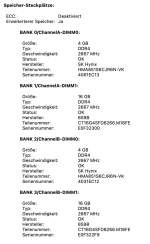
Memory Device #: 0
==============
Total Width: 72 bits
Data Width: 64 bits
Size: 8192 MB
Form Factor: DIMM
Device Set: 1
Device Locator: DIMM1
Bank Locator:
Memory Type: DDR3
Type Detail: Synchronous
Speed: 1866 MT/s
Manufacturer: 0x80CE
Serial Number: 0x13515C02
Asset Tag: Unknown
Part Number: 0x4D33393342314737305148302D434D412020
Attributes: 00000000
Configured Memory Speed: N/A
Minimum Voltage: N/A
Maximum Voltage: N/A
Configured Voltage: N/A
Memory Technology: Unknown
Memory Operating Mode Capability: Unknown
Firmware Version:
Module Manufacturer ID: N/A
Module Product ID: N/A
Memory Subsystem Controller Manufacturer ID: N/A
Memory Subsystem Controller Product ID: N/A
Non Volatile Size: N/A
Volatile Size: N/A
Cache Size: N/A
Logical Size: N/A
Memory Device #: 1
==============
Total Width: 72 bits
Data Width: 64 bits
Size: 8192 MB
Form Factor: DIMM
Device Set: 1
Device Locator: DIMM2
Bank Locator:
Memory Type: DDR3
Type Detail: Synchronous
Speed: 1866 MT/s
Manufacturer: 0x80CE
Serial Number: 0x13515B30
Asset Tag: Unknown
Part Number: 0x4D33393342314737305148302D434D412020
Attributes: 00000000
Configured Memory Speed: N/A
Minimum Voltage: N/A
Maximum Voltage: N/A
Configured Voltage: N/A
Memory Technology: Unknown
Memory Operating Mode Capability: Unknown
Firmware Version:
Module Manufacturer ID: N/A
Module Product ID: N/A
Memory Subsystem Controller Manufacturer ID: N/A
Memory Subsystem Controller Product ID: N/A
Non Volatile Size: N/A
Volatile Size: N/A
Cache Size: N/A
Logical Size: N/A
Memory Device #: 2
==============
Total Width: 72 bits
Data Width: 64 bits
Size: 16384 MB
Form Factor: DIMM
Device Set: 1
Device Locator: DIMM3
Bank Locator:
Memory Type: DDR3
Type Detail: Synchronous
Speed: 1866 MT/s
Manufacturer: 0x80AD
Serial Number: 0x186A6447
Asset Tag: Unknown
Part Number: 0x484D54343247523741465234432D52442020
Attributes: 00000000
Configured Memory Speed: N/A
Minimum Voltage: N/A
Maximum Voltage: N/A
Configured Voltage: N/A
Memory Technology: Unknown
Memory Operating Mode Capability: Unknown
Firmware Version:
Module Manufacturer ID: N/A
Module Product ID: N/A
Memory Subsystem Controller Manufacturer ID: N/A
Memory Subsystem Controller Product ID: N/A
Non Volatile Size: N/A
Volatile Size: N/A
Cache Size: N/A
Logical Size: N/A
Memory Device #: 3
==============
Total Width: 72 bits
Data Width: 64 bits
Size: 16384 MB
Form Factor: DIMM
Device Set: 1
Device Locator: DIMM4
Bank Locator:
Memory Type: DDR3
Type Detail: Synchronous
Speed: 1866 MT/s
Manufacturer: 0x80AD
Serial Number: 0x187A644F
Asset Tag: Unknown
Part Number: 0x484D54343247523741465234432D52442020
Attributes: 00000000
Configured Memory Speed: N/A
Minimum Voltage: N/A
Maximum Voltage: N/A
Configured Voltage: N/A
Memory Technology: Unknown
Memory Operating Mode Capability: Unknown
Firmware Version:
Module Manufacturer ID: N/A
Module Product ID: N/A
Memory Subsystem Controller Manufacturer ID: N/A
Memory Subsystem Controller Product ID: N/A
Non Volatile Size: N/A
Volatile Size: N/A
Cache Size: N/A
Logical Size: N/A
")
")